- 您现在的位置:买卖IC网 > Sheet目录1993 > DS1254WB-150 (Maxim Integrated Products)IC NVSRAM 16MBIT 150NS 168BGA
DS1254
7 of 17
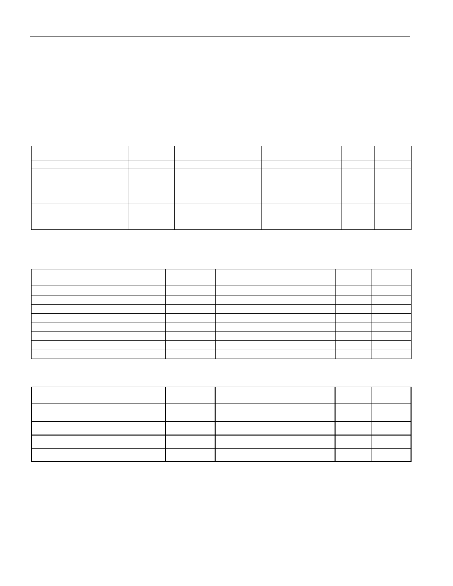
ABSOLUTE MAXIMUM RATINGS
Voltage Range on Any Pin Relative to Ground
-0.3V to +4.6V
Operating Temperature Range
0
C to +70C
Storage Temperature Range
-40
C to +70C
Soldering Temperature
See IPC/JEDEC J-STD-020
Stresses beyond those listed under “Absolute Maximum Ratings” may cause permanent damage to the device. These are stress ratings only,
and functional operation of the device at these or any other conditions beyond those indicated in the operational sections of the specifications is
not implied. Exposure to the absolute maximum rating conditions for extended periods may affect device.
RECOMMENDED DC OPERATING CONDITIONS
(TA = 0
C to +70C)
PARAMETER
SYMBOL
CONDITIONS
MIN
TYP
MAX
UNITS
NOTES
Power-Supply Voltage
VCC
3.0
3.3
3.7
V
1
Logic 1 Voltage (All Inputs)
VIH
2.0
VCC +
0.3
V
1
Logic 0 Voltage (All Inputs)
VIL
-0.3
0.6
V
1
DC ELECTRICAL CHARACTERISTICS
(VCC = 3.3V 10%, TA = 0
C to +70C.)
PARAMETER
SYMBOL
MIN
TYP
MAX
UNITS
NOTES
Input Leakage Current
IIL
-4.0
+4.0
A
I/O Leakage Current
IIO
-4.0
+4.0
A
Output Current at 2.4V
IOH
-1.0
mA
3
Output Current at 0.4V
IOL
2.0
mA
3
Standby Current (
CE = 2.2V)
ICCS1
5.0
7
mA
Standby Current (
CE = V
CC - 0.5V)
ICCS2
2.0
3.0
mA
Operating Current, tCYC = 100ns
ICCO1
50
mA
Write Protection Voltage
VPF
2.8
2.97
V
1
CAPACITANCE
(TA = +25
C)
PARAMETER
SYMBOL
MIN
TYP
MAX
UNITS
NOTES
Input Capacitance: A0 to A18,
OE,
WE, CE
CIN
25
50
pF
Input Capacitance: A19 to A20
CIN
5
10
pF
I/O Capacitance: DQ0 to DQ7
CIO
25
50
pF
Output Capacitance:
BW
COUT
5
10
pF
发布紧急采购,3分钟左右您将得到回复。
相关PDF资料
DS1286I+
IC TIMEKEEPER WATCHDOG 28-EDIP
DS12885T
IC RTC W/RAM 128 BYTE 32-TQFP
DS12C887A+
IC RTC W/RAM 128 BYTE 24-EDIP
DS12CR887-5+
IC RTC W/RAM 128 BYTE 24-EDIP
DS1302SN-16
IC TIMEKEEPER T-CHRG IND 16-SOIC
DS1305E/T&R
IC RTC SERIAL ALARM 20-TSSOP
DS1306EN/T&R
IC RTC SERIAL ALARM IND 20-TSSOP
DS1307N
IC RTC SERIAL 512K IND 8-DIP
相关代理商/技术参数
DS1254WB2-150
功能描述:实时时钟 2M X 8 NV SRAM w/Phantom Clock RoHS:否 制造商:Microchip Technology 功能:Clock, Calendar. Alarm RTC 总线接口:I2C 日期格式:DW:DM:M:Y 时间格式:HH:MM:SS RTC 存储容量:64 B 电源电压-最大:5.5 V 电源电压-最小:1.8 V 最大工作温度:+ 85 C 最小工作温度: 安装风格:Through Hole 封装 / 箱体:PDIP-8 封装:Tube
DS1254WB-C01
功能描述:实时时钟 2M X 8 NV SRAM w/Phantom Clock RoHS:否 制造商:Microchip Technology 功能:Clock, Calendar. Alarm RTC 总线接口:I2C 日期格式:DW:DM:M:Y 时间格式:HH:MM:SS RTC 存储容量:64 B 电源电压-最大:5.5 V 电源电压-最小:1.8 V 最大工作温度:+ 85 C 最小工作温度: 安装风格:Through Hole 封装 / 箱体:PDIP-8 封装:Tube
DS1254WB-C02
功能描述:实时时钟 2M X 8 NV SRAM w/Phantom Clock RoHS:否 制造商:Microchip Technology 功能:Clock, Calendar. Alarm RTC 总线接口:I2C 日期格式:DW:DM:M:Y 时间格式:HH:MM:SS RTC 存储容量:64 B 电源电压-最大:5.5 V 电源电压-最小:1.8 V 最大工作温度:+ 85 C 最小工作温度: 安装风格:Through Hole 封装 / 箱体:PDIP-8 封装:Tube
DS1254YB-100
功能描述:IC NVSRAM 16MBIT 100NS 168BGA RoHS:否 类别:集成电路 (IC) >> 时钟/计时 - 实时时钟 系列:- 产品培训模块:Obsolescence Mitigation Program 标准包装:1 系列:- 类型:时钟/日历 特点:警报器,闰年,SRAM 存储容量:- 时间格式:HH:MM:SS(12/24 小时) 数据格式:YY-MM-DD-dd 接口:SPI 电源电压:2 V ~ 5.5 V 电压 - 电源,电池:- 工作温度:-40°C ~ 85°C 安装类型:表面贴装 封装/外壳:8-WDFN 裸露焊盘 供应商设备封装:8-TDFN EP 包装:管件
DS1254YB2-100
功能描述:实时时钟 2M X 8 NV SRAM w/Phantom Clock RoHS:否 制造商:Microchip Technology 功能:Clock, Calendar. Alarm RTC 总线接口:I2C 日期格式:DW:DM:M:Y 时间格式:HH:MM:SS RTC 存储容量:64 B 电源电压-最大:5.5 V 电源电压-最小:1.8 V 最大工作温度:+ 85 C 最小工作温度: 安装风格:Through Hole 封装 / 箱体:PDIP-8 封装:Tube
DS125-6-2G
制造商:Electronic Hardware Corporation (EHC) 功能描述:CRANK HANDLE ROUND KNOB 6.35MM 制造商:EHC (ELECTRONIC HARDWARE) 功能描述:CRANK HANDLE ROUND KNOB, 6.35MM 制造商:EHC (ELECTRONIC HARDWARE) 功能描述:CRANK HANDLE ROUND KNOB, 6.35MM; Knob / Dial Style:Round with Crank Handle; Shaft Diameter:6.35mm; Knob Diameter:31.75mm; Shaft Type:Round; Knob Material:Plastic; Shaft Size:1/4 (6.35) in. (mm) ;RoHS Compliant: Yes
DS1258AB-100
功能描述:NVRAM
RoHS:否 制造商:Maxim Integrated 数据总线宽度:8 bit 存储容量:1024 Kbit 组织:128 K x 8 接口类型:Parallel 访问时间:70 ns 电源电压-最大:5.5 V 电源电压-最小:4.5 V 工作电流:85 mA 最大工作温度:+ 70 C 最小工作温度:0 C 封装 / 箱体:EDIP 封装:Tube
DS1258AB-100#
功能描述:NVRAM
RoHS:否 制造商:Maxim Integrated 数据总线宽度:8 bit 存储容量:1024 Kbit 组织:128 K x 8 接口类型:Parallel 访问时间:70 ns 电源电压-最大:5.5 V 电源电压-最小:4.5 V 工作电流:85 mA 最大工作温度:+ 70 C 最小工作温度:0 C 封装 / 箱体:EDIP 封装:Tube